Piercing Pin
APPLICATION: Exposure optical imaging graphic transfer special positioning nails in double/multi-layer printed circuit board. TOLERANCE: +0.005/-0.02mm SHAPE: pointed-end with four sides open SPECIFICATION: Φ5.0×1.2×3.1 Φ5.0×1.5×Φ3.0 Φ5.0×1.5×Φ3.15 Φ6.0×1.4×Φ3.1 Φ6.0×1.45×Φ3.15 Φ6.0×1.45×Φ3.175
Filtering...
Abrasive ...
Cleaning ...
Ceramic B...
Sticky Pa...
Titanium ...
EMI Shiel...

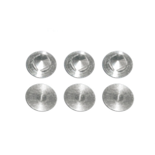


APPLICATION: Exposure optical imaging graphic transfer special positioning nails in double/multi-layer printed circuit board.
TOLERANCE: +0.005/-0.02mm
SHAPE: pointed-end with four sides open
SPECIFICATION: Φ5.0×1.2×3.1
Φ5.0×1.5×Φ3.0
Φ5.0×1.5×Φ3.15
Φ6.0×1.4×Φ3.1
Φ6.0×1.45×Φ3.15
Φ6.0×1.45×Φ3.175